XP2 Board: Clock, Power and Reset Subsystems

Power Supply Subsystem

The XP2 Brevia Board is powered by an AC adapter connected on J6 jack.  The AC adapter converts the AC voltage to a 6V, 1 A DC voltage.  This DC input is then fed into two National LM117 voltage regulators.  According to the LM117 data sheet, the out voltage ranges from 1.2 to 37 at 1.5 A and is configurable using resistors in the output feedback loop.  The output is computed using the following equation:

Vout = Vref (1 + R2/R1) + Iadj*R2

As per the data sheet, Vref is a fixed 1.25 V, and Iadj is a small fixed current.  In the equation above, the Iadj part is small enough to be ignored for practical purposes.  For the 1.2 V output, “R2” is R22, a zero ohm resistor, and thus the output voltage is equal to Vref.  This is within the tolerance of the FPGA core voltage, the input voltage required to power the core parts of the FPGA: the LUTs, flip-flops, mux, etc. that make up the logic cells.

For the 3.3 V output, “R2” is R24 and “R1” is R23.  R2/R1 is 1.65, which when added to 1 and multiplied by Vref provides about 3.3V volts.  This 3.3V is actually Vio, the voltage required for the FPGA input and output pads.  Most FPGAs usually have two voltage supplies: the core and I/O voltages.  FPGAs with high speed serial transceivers–SERDES–often have a separate supply for these transceivers.

On the schematic also note the capacitors C26-C32 and C37-C45 placed respectively between the 1.2V and 3.3V regulated output and ground.  C27-C45 are shown below as in the schematic.

These are decoupling capacitors, usually inserted between an IC voltage input and ground so that when the IC draws large currents and the voltage supply level temporarily drops, the capacitors discharge their stored energy in and effort to keep the voltage level constant.  The capacitors are often drawn this way in industry so as not to clutter the schematic near the ICs.  This style does make it easier for FPGA, micro-controller, or microprocessor developers to focus on the I/Os around the device.

Another interesting section of the schematic on the page with the DC regulators is the ground-ground connection:

Often this is a notation to mark that the digital and analog ground planes are to be joined by a connection so that both analog and digital share the same ground plane.

Clock Subsystem

A 50 MHz square wave output oscillator (select the H22/H32/H53/SWO datasheet), X1, is on the circuit board and will act as the reference clock in the FPGA.  The output of the oscillator, XOUT, is directly connected to the FPGA and there is not really anything interesting in this clock subsystem, except for C8 attached between the XOUT signal and ground.  C8 is a load capacitor, and for  more information on load capacitors on the output of an oscillator, consult the manufacturer’s technical note Effect of Load Capacitance on the Crystal.

We will do more with the clock signal once we start working with the innards of the FPGA.

Global Reset Subsystem

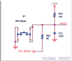
The XP2 board has a reset push-button, S1, that when pushed resets the FPGA to an initial state.  The circuit for the reset is shown below:

The circuit attached to the output of the push-button S1 is a simple analog debouncing circuit.  A debounce circuit is necessary because it prevents spurious noise from accidentally resetting the system.  Conceptually, the debounce circuit is very easy to understand.  When 3.3V is supplied and the push-button is depressed, the RESET and signal is a logical ‘high’ or ‘1’ value, and capacitor C13 begins to charge.  Remember that the time required for the capacitor to discharge is roughly 5*T, where T=R19*C13.  When the push button is pressed it causes the current from 3.3V to travel the path of least resistance to ground.  In other words, the RESET signal is pulled-down to ground.  Capacitor C13 resists voltage changes, and starts to discharge its stored energy in an futile attempt to keep the voltage levels the same.  After about 5*T, the capacitor will be completely discharged and RESET sits at ‘low’ or ‘0’ value.  The following is a simple SPICE (MacSpice) model that shows the level of RESET: the switch is initially open, and then at t=1ms the push-button is pressed and held down.

* Analog Switch Debouncing
* Use a pulse to emulate the behavior of an analog switch pulling-down input voltage
V1 1 0 PULSE(0 3.3 2ns 2ns 2ns 1ms 2ms)
R1 1 2 10k
C1 2 0 10n ic=0
.control
tran .005 .002 uic
plot v(2)
.endc
.end

V(2) is the equivalent of the RESET signal in the circuit schematic above.

Because the push-button must be depressed longer than 5*T, sudden spikes and instantaneous signals on the RESET line will not cause the FPGA to be reset.  For this circuit, under ideal circumstances, T=10k*10nF=100us, and 5*T is 500us.  For modern FPGAs and digital circuits, 500us is an eternity!  Only a purposeful reset will make its way to the FPGA.  Note also that the signal XP2_RESET is connected to RESET by a zero ohm resistor R20.  XP2_RESET goes to the external connector J4 pin 39 so that an FPGA on one board will travel to any external connections to J4.  XP2_RESET can be disabled by removing R20 from the circuit board if desired.

Conclusion

Now that we understand the power, clock and reset sub-systems, we are ready to begin experimenting with the FPGA itself.  The next step is to setup the clock and reset signals inside of the FPGA.

XP2 Board: JTAG scan with ispVM

Back in business, and ain’t it grand! So I decided to go with option number two and bring my old PC back to life. I could not stand the though of having to reboot between Mac OS X and Windows.  With the old PC I have not tried to build any designs or run any simulations yet, but the machine should be able to handle it, perhaps quite slowly though.

To continue with my exploration of the XP2 board, I thought it best to make sure that I could see the FPGA in the JTAG programming chain.  JTAG is an simple interface used for testing silicon devices on a circuit board, and it is also a common interface for programming FPGAs during the design and testing phase in the development cycle.  Every FPGA vendor has its own tool for programming devices, and for Lattice FPGAs the tool is ispVM.

Lets get started.  First the XP2 board must be connected to a JTAG programming cable using the J3 connector labeled “JTAG” on the circuit board.  For the parallel port programming cable supplied with the XP2 Brevia Kit, just follow the directions in the QuickStart guide.  For the USB programming cable, note the the names of the different wires, and then use the QuickStart guide to match the wire name to the right pin.

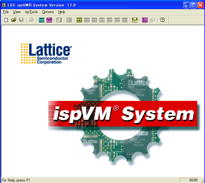
Once the cable is connected correctly, supply power to the XP2 board and launch ispVM.  After it opens, I like to close all of the open windows in the GUI and start fresh, as shown below.

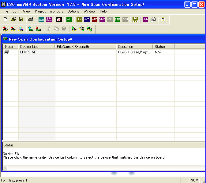
To perform a simple JTAG chain scan, press F2 or select from the menu bar ispTools->Scan Chain.  ispVM reports all of the devices in the JTAG chain connected to connector J1 on the board. For this XP2 Brevia board, the only device is the XP2 FPGA itself.  In more complex designs, it is not uncommon to have several devices in the chain, such as a flash memory for device configuration, FPGAs, CPLDs, and even embedded processors like PowerPC or DSPs.  When the scan is complete, the XP2 FPGA should be visible and the only device:


XP2 FPGA found from the JTAG chain scan

As expected, the device is visible and we have also gained some basic familiarity with the ispVM tool.  With both the serial port verified with the demo program and the JTAG scan completed, the basic connections to the outside world are verified.  Before creating a simple design and programming it to the device, there is one more critical step that requires attention: power and clock systems on the circuit board.  And that shall be the topic of the next post!

Regarding my XP2 posts

I have found that I am going to have to pause my series on the XP2 board.  The reason is that I cannot get my USB programmer to be recognized by Lattice’s software via VirtualBox.  I use Mac OS X, and I have Windows XP2 installed in a virtual machine (VirtualBox).  Though Mac OS X recognizes the USB programmer and VirtualBox does as well, Lattice’s software does not recognize the hardware and nor does Windows XP.  I cannot seem to find a way to get it to either, so I’m essentially dead in the water.

At this point I have three options:

  1. Install BootCamp on my Mac so that I can dual boot OS X and Windows XP — I don’t particularly like this because the Windows XP install will eat up quite a bit of my disk space that I would rather use for video editing.  I suppose I could reclaim some of it by deleting my VirtualBox Windows XP install. But I hate the idea of having to reboot to use Windows or Mac OS X, what a pain!  Hopefully a native install of Window with direct access to the USB subsystem on this computer would allow the Lattice USB programmer to function.
  2. I have an old Pentium-III machine with 256 MB of memory and 10 GB of disk space that runs Windows 2000 smoothly.  I do not have a monitor for the machine, however, so I would need to purchase a monitor, then setup the machine again, and hope that the Lattice software won’t overpower this old machine that I purchased in 1999.  This machine has a parallel port on the motherboard, so I could use the parallel port programmer cable that came with the XP2 board.  This parallel port support gives me some hope that Lattice’s design software is no overbearing. After all, new Dell PCs don’t even have parallel ports!
  3. Buy a new PC with Windows 7 – I’d rather not take this route, but for the long-term it may be necessary.  My hobby and passion is electronics, and despite how much I love Mac OS X, I may have to prepare a Windows machine so that I can take advantage of all of the free tools available for Windows in the electronics world.  I could purchase a basic modern PC for less than $400 and I could get a nice monitor for $200, but that is still a lot of money when I am already happy with my Mac.

Decisions, decisions, decisions.  Once I’ve found my solution I will re-start this series about the Lattice XP2 board.  In the mean time, I have learned that despite the growth in Mac computing, Windows still rules the world.  Even though most of the FPGA vendors now support Linux, I would still go the Windows route until the industry is ready to accept Linux alongside Windows.

Software access to XP2 board

Thanksgiving has come and gone and my life is back to the usual schedule.  That means I have time to experiment with my XP2 board!  In my last post I made sure that I could access the XP2 board from a terminal.  I now want to do this in a programmable way with software. Instead of using a standard terminal interface, my long-term plan is to use a binary serial protocol to communicate between my PC software and the FPGA on the XP2 board.

I coded up some simple C language functions that access and perform I/O via the serial port using standard POSIX functions.  It was simple and did not require much effort, and I’m left wondering why if serial ports can be supported for Linux, why other POSIX platforms like Mac OS X have no support.  I suppose the GNAT supporters have their reasons…probably due to business “use cases”.

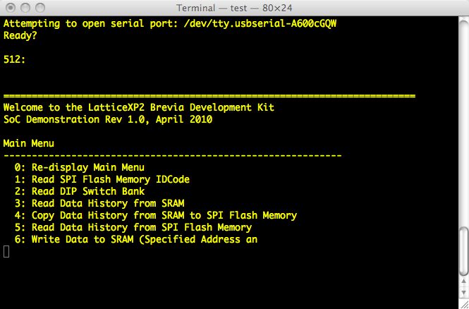
Nonetheless, using standard POSIX interfaces worked fine on Mac OS X.  For example, the following screen capture shows the result of reading 512 bytes from the serial port after resetting the XP2 board:

The output matches the terminal output I captured last time with the screen program, and my simple C code serves to prove that we are ready on the software side to interact with theXP2 board.  I will not publish the C code just yet–I plan to make it more adaptive and provide an Ada interface as well.  Just using C would be no fun, I’d learn nothing new.  But interfacing C and Ada, especially since GNAT does not provide serial port support for OS X, is  a great opportunity to learn more about Ada.

My USB programmer cable arrived in the mail recently, and now that we have the software interface working as expected, it is time to make sure the JTAG interface on the hardware works as expected.  Once we have the JTAG programmer figured out, we can try to implement some simple logic in the FPGA.

Connecting to the XP2 Brevia Board

Much to my surprise, my Lattice XP2 Brevia board arrived in the post today.  I printed out the User’s Guide with the schematic because I know I’ll be pouring over the schematics during my lunch break at work and when I get home in the evenings.  The kit contains a null-modem (serial port) cable, the 3 inch x 2 inch board, a parallel-port programming cable, and a power adapter with exchange sockets depending on the electrical standard in your region.  This is truly a versatile development kit for experimenting with FPGAs.

Because I don’t have a PC with a built in parallel port, I have to use a USB programmer, and I’m still waiting on my Lattice USB programming cable to arrive in the post.  Note: Lattice says that USB-to-parallel converters will not work with their parallel port programming cable.

It is often helpful to evaluate the status of the board before beginning with prototyping and development.  If I had designed the board myself, I would be checking the voltage levels at critical parts in the circuit and making sure they match they intended levels.  I’d also be checking the power-up sequence and reset circuits to make sure that these basic functions behave as expected.  I trust, however, that Lattice has taken care of this.

My test plan is:

  1. Connect to the board’s serial interface via a terminal and verify that the factory-installed demo application runs as expected
  2. Connect to the board’s serial interface with my own software and make sure I can interact with the factory-installed demo application

Connecting to the board with a terminal

If you have a Microsoft Windows workstation, you can follow the Lattice QuickState guide and use HyperTerminal to connect to the board.  Though I have Windows installed through a Virtual Machine, I only use it for the Lattice FPGA design software and device programmer.  I would like to use my preferred OS, Mac OS X, for interacting with the XP2 board.  While Mac OS X does not have a graphical application like Microsoft’s HyperTerminal pre-installed, we can use a terminal tool called screen.

Screen comes installed on Mac OS X and it is accessible via the terminal (of course).  The Lattice QuickStart guide says that the serial connection parameters are 8 data bits, no parity, 1 stop bit, no flow control and a baud rate (bits per second) or 115,200.  Most of the parameters, except for the baud rate, are rather standard, so I just have to specify the baud rate when I start a new screen session.

screen /dev/tty.usbserial-A600cGQW 115200

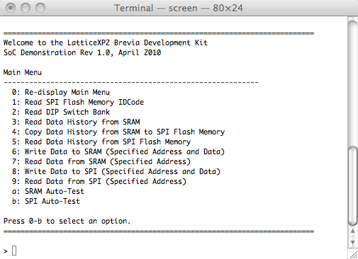
Now I just have to press the reset button on the XP2 board:

Voila!  I am now hooked up to the factory-installed demo application.  Next I will use some custom C software and make sure I can interact with the demo application.